NVIDIA A100 - the most powerful Ampere accelerator will see a version with a PCIe connector and 80 GB of HBM2e memory
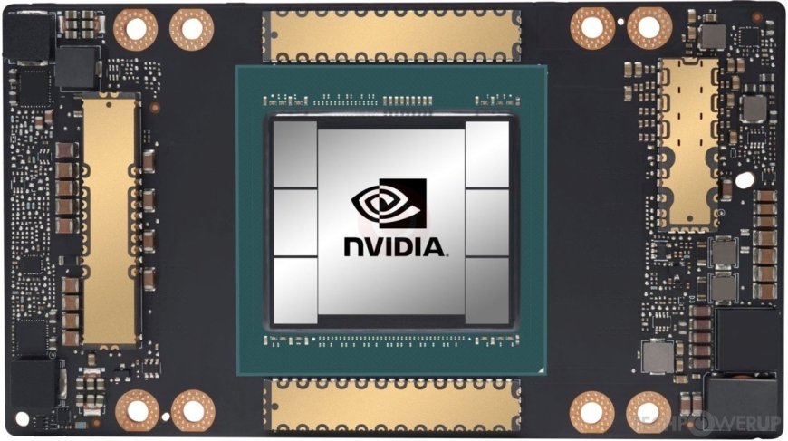
In May 2020, NVIDIA presented the capabilities of the new Ampere architecture for the first time at a special event organized as part of the GPU Technology Conference. It started with the largest and most efficient single chip in the form of the A100 accelerator, used for specialized HPC calculations and based on artificial intelligence. A month later, the manufacturer introduced the A100 in the PCIe version (previously only in the form of the SXM module) - both variants initially offered 40 GB of HBM2e memory, although after a few months the NVIDIA A100 SXM also appeared with 80 GB of memory. The PCIe variant, although less power hungry, was only offered with 40 GB VRAM. This will change soon, because the company's documentation shows that another version of the accelerator for PCIe is planned, in an even more extensive version.
NVIDIA will soon introduce the A100 graphics accelerator, based on the Ampere architecture (GA100) and offering 80 GB of memory on the PCIe connector.
Must Read: Petition filed in the Supreme Court for ban on Tik tok
The NVIDIA A100 PCIe chip is based on TSMC's 7nm process technology. The Ampere GA100 graphics core itself also has a much larger surface area of ‹‹826 mm², which makes it a gigantic chip. Ampere GA100 includes, among others 54 billion transistors, although the variant presented so far has been equipped with 6912 CUDA cores and 108 active SM blocks (Streaming Multiprocessor). So it is not a full core that offers 128 SM blocks and 8192 CUDA cores. The first version of the A100 chip with the PCIe 4.0 bus had 40 GB of HBM2e memory with a total bandwidth of 1555 GB / s.
Although NVIDIA has not yet officially disclosed this information, the website mentions a new version of the A100 accelerator, which not only uses the PCIe 4.0 bus, but also has twice as much memory - 80 GB HBM2e, with even higher bandwidth, reaching 2 TB / s. It will therefore be one of the most advanced accelerators for professional tasks. Currently, the documentation only specifies the larger VRAM size. We do not know whether the core configuration itself will remain the same, or whether NVIDIA will finally be tempted to introduce a full Ampere GA100 chip with 8192 CUDA cores.